Frequently Asked Questions
Our goal is to be responsive to the needs of our customers by supplying the highest possible quality products on time with the best possible pricing and value.
5.0V Clock required - Use 3.3V CMOS Clock
The 5V CMOS clock oscillators are declining in availability. This is a solution to use the readily available 3.3V clock oscillators.
The Pletronics SM33xxT, SM44xxT, SM55xxT, SM77xxH and SM77xxD families of 3.3V oscillators can be used with this circuit to fulfill the need for a 5.0V clock oscillator. The resulting signal characteristics will be equal to or better than the older 5V clock oscillators.

Ceramic Packaged Oscillators with "S" in the PN
As technology improved for the integrated circuits used to make the oscillators, the standard specification was updated to 45% to 55% without any testing or screening. All ceramic packaged oscillators from Pletronics meet this 45% to 55% duty cycle.
Since the “S” had no official meaning, this was dropped from all part numbers for ceramic parts. Therefore as an example: the SM7745HSV-25.0M is the same as the SM7745HV-25.0M and both parts have a 45% to 55% duty cycle.
Part numbers with the “S” in them are accepted as a legacy part number but have no special meaning.
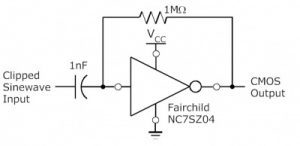
Converting Clipped Sinewave Output to CMOS
Clipped Sinewave output signal from many TCXO’s and other oscillators is easily converted to a CMOS output signal.
This simple circuit can be driven by the oscillators rated for 0.8V PP clipped sinewave output specified to have a maximum load of 10K ohm in parallel with 10pF. The output will have a CMOS square wave with a Vcc PP level and close to a 50% duty cycle.
This circuit will work from 1.65V to 5.5V and to over 70MHz at the lowest supply voltage.
Deterministic Jitter
The predictable component of jitter is called deterministic jitter. For non multiplied quartz crystal oscillators the deterministic jitter is typically less than 0.01pS. Additional information on jitter can be found in our Docs/PCN/EOL section under Helpful Documents from Pletronics.
Fine Leak Testing Criteria
Helium Bombing Soak time : 7200sec(2hrs)
Bombing pressure : 75psig
Reject Criteria:
>5.00-8 atm.cc/sec
LVDS driving mutliple inputs
http://www.xilinx.com/support/documentation/application_notes/xapp231.pdf
Part Marking Information
Phase Noise to Jitter Conversion
Shock level and broken crystals causing failures
The crystal inside the package is suspended in free space inside the package, suspended in dry nitrogen or in an evacuated space. A high shock can cause the the precision timing element to fracture.
Most of the Pletronics products are rated to 1500Gs, this level of shock can be easily reached by dropping the device on the floor.
This chart shows the G force reached when dropping an object on a hardwood or a vinyl type floor surface. The forces are much higher on a concrete floor.

Suggesting PCB/PWB pad geometries
Previously the whole electronics industry was using lead tin solder and Pletronics could make recommendations based on this consistent requirement. Today, we have many different processes, many different fluxes, many differing process temperatures.
Add to this complexity that there are concerns about the resulting chemistry of the solder joint. For example, our ceramic crystals and oscillators have gold plating on the nickel pads to assure solderability, for some end users there is concern about the resulting concentration of gold in the completed solder joint.
The end user has to make the decision on what makes their process perform reliably, while considering the Pletronics pads, the PCB/PWB pad size, any plating on the PCB/PWB and the thickness of the solder screens.
Pletronics does provide accurate package pad information on the datasheets to assist in determining the proper PCB/PWB design.
Symmetry - Why only 45/55%?
Question – What is the difference between standard CMOS oscillator symmetry of 40/60% and the special specification of (S) 45/55% symmetry?
Answer – 45/55% symmetry is tighter than 40/60%. Most of our oscillators will work at both 40/60% and 45/55% symmetry regardless of marking.
Total Jitter
Total jitter is is the sum of Deterministic Jitter and Random Jitter.
For non multiplied crystal oscillators (oscillators using fundamental mode or thrid overtone crytals), the deterministic jitter is typically less than 0.01pS.
Additional information on jitter can be found in our Docs/PCN/EOL section under Helpful Documents from Pletronics.
Why do TCXOs have clipped sinewave outputs?
* CMOS output would add significant power dissipation to the TCXO IC. The resulting temperature gradients on the IC and in the package would limit the ability to achieve the best TCXO compensation.
* The wide range of possible CMOS loads would alter the compensation design as internal thermal gradients result in the TCXO not meeting specifications.
* CMOS outputs result in power supply and ground transients when the output is changing levels. This noise would adversely affect the phase noise performance of the TCXO.
* CMOS outputs generate much larger EMI/RFI signals that can result in difficulties meeting the USA FCC and other countries radiated energy limits from the final system. The clipped sinewave, being both low amplitude and mostly sinusoiddal, results in low signal levels and less harmonics.
* Many of the applications where these TCXOs are used have ASIC inputs that accept the clipped sinewave and convert to CMOS logic levels internally.
See our FAQ about converting clipped sinewave levels to CMOS. It is easy to do and low cost.
Why does a crystal have a lower frequency limit?
An 8MHz crystal would be 0.0078″ (0.200mm) thick. A 4MHz crystal would be 0.0157″ (0.400mm) thick.
Two conditions are encountered that limit the lowest frequency in a particular size of package:
1) The simple condition, the newer low profile ceramic LCC packages will not accept the thicker crystals. Depending on the package, the lower frequency limits range from 8MHz to 12MHz and downward.
2) Remember that a quartz crystal is a vibrating mechanical device. For the best designs, those with lower ESR (CI) and no perturbations (undesired modes of vibration that cause frequency jumps) the vibrating area is intended to be in the center area of the crystal.
When the crystal frequency is lower and the crystal is thicker, the vibrating area is more mechanically coupled to the edges. In this case the perturbations (unwanted resonances) become difficult to nearly impossible to control. The solution is to bevel or contour the crystal (make the crystal look more like a magnifying glass concave shape). This thinning of the edges restricts the vibrating area to the crystals center and allows control of the perturbations.
Unfortunately, restricting the vibrating area increases the ESR significantly. For example at 12MHz:
SM13T 5x7mm crystal ESR maximum is 50 ohms
SM11T 3.2x5mm crystal ESR maximum is 80 ohms
For this example, an SM11T below 12MHz is not practical as the ESR becomes very large.